会议简介
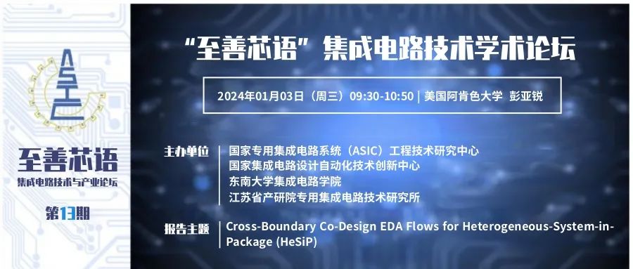
“至善芯语”论坛第13期邀请到了美国阿肯色大学计算机科学和计算机工程助理教授彭亚锐做学术报告,会议将于1月3日(周三)上午9:30在EDA国创中心5楼501会议室举办,线上腾讯会议同步进行,欢迎各位行业同仁参与、交流和学习。
主办单位
国家专用集成电路系统(ASIC)
工程技术研究中心
国家集成电路设计自动化技术创新中心
东南大学集成电路学院
江苏省产研院专用集成电路技术研究所
时间与地点
2024年01月03日(周三)
09:30-10:50
EDA国创中心
5楼501会议室
报告人
美国阿肯色大学 彭亚锐
报告主题
Cross-Boundary Co-Design EDA Flows for Heterogeneous-System-in-Package (HeSiP)
腾讯会议号
430-811-598
嘉宾介绍
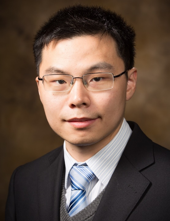
美国阿肯色大学
助理教授 彭亚锐
Yarui Peng received the B.S. degree from Tsinghua University, Beijing, China in 2012. He earned his M.S. degree and Ph.D. in School of Electrical and Computer Engineering from Georgia Institute of Technology, Atlanta, USA in 2014 and 2016, respectively. He is an Assistant Professor in Computer Science and Computer Engineering at the University of Arkansas. He also collaborates with the NSF Engineering Research Center for Power Optimization of Electro-Thermal Systems and the UA Power Group.
His research interests are in the areas of computer-aided design, analysis, and optimization for emerging technologies and systems, such as 2.5D and 3D ICs, high band-gap power electronics and systems, and high-efficiency digital designs and memory systems. He developed methodologies and algorithms for parasitic extraction, analysis and optimization for signal integrity, and alleviating reliability issues in thermal and power delivery in 2.5D and 3D ICs. He is also working on improving electro-thermal reliability in power systems such as multi-chip power modules (MCPMs). He is the recipient of best-in-session award in SRC TECHCON 14 and best student paper award in ICPT 16. He received NSF CAREER Award in 2021.
报告摘要
In recent days, chiplet and advanced packaging have gained popularity with an increasing number of heterogeneous designs integrated into advanced system-in-packages. This trend presents a growing impact on system performance, reliability, and integrity. At present, there exists no standard EDA flow that can design, analyze, and optimize complete heterogeneous 2.5D/3D chiplet-based systems. The traditional die-by-die design approach processes each component independently during extraction and optimization and cannot be applied to heterogeneous systems without fundamental changes in standard CAD tools.
I will present a complete chiplet-package co-optimization flow for both homogeneous and heterogeneous 2.5D designs. It encompasses 2.5D-aware partitioning, chiplet-package co-planning, holistic and in-context extraction, package inductance consideration, and iterative optimization, along with design analysis and verification of the entire 2.5D system. For homogeneous 2.5D packages, the performance gap to the reference 2D design reduces by 62.5% with our holistic flow. Targeting heterogeneous systems, our in-context design flow achieves less than 1% extraction error on ground and coupling capacitance with comparable design performance. We also develop our extraction and analysis tool that accurately models RDL wire inductive timing and noise impact and allows ASIC design tools to optimize the design using our 2.5D design framework.
In addition, Heterogeneous-System-in-Package (HeSiP) further enables integrating mixed-signal and even non-Si chiplets, such as IO/PHY, MEMS, PMIC, and Wide Bandgap (WBG) Power Electronics. EDA tools, models, and algorithms for heterogeneous integration are essential enabling technologies. With the adoption of wide-bandgap semiconductors (e.g., SiC, GaN), the next-generation power converters are on the horizon. Research on design automation and optimization has been identified as an emerging topic in the power electronics society.
I will present the latest design automation flow for high-density (2D/2.5D/3D) and heterogeneous multi-chip power modules (MCPM) through PowerSynth 2 framework. We demonstrate electrothermal optimization for SOTA 3D Power Packaging technologies and present the path towards signal-energy co-design. This further extends the layout synthesis process and multi-objective design methodologies for heterogeneous chiplet integration beyond Si and CMOS.